
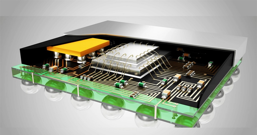
As semiconductor technology advances to meet the demands of AI, high-performance computing and mobile applications, monolithic 3D integration is emerging as a game-changing innovation in chip packaging. Unlike traditional 3D stacking, which relies on Through-Silicon Vias (TSVs) and micro-bump interconnects, monolithic 3D integration enables transistor-level vertical stacking within the same wafer, significantly improving performance, power efficiency and scalability. Erik Hosler, a specialist in advanced metrology techniques and semiconductor innovation, recognizes the importance of precision in fabrication techniques in ensuring that monolithic 3D integration can drive next-generation semiconductor efficiency.
Why Monolithic 3D Integration is a Breakthrough
The limitations of traditional scaling methods drive the shift toward monolithic 3D integration. While Moore’s Law has historically dictated the pace of transistor miniaturization, conventional 2D scaling is reaching physical and economic barriers. Monolithic 3D integration overcomes these challenges by stacking active transistor layers directly on top of one another, reducing interconnect lengths and signal delay while dramatically improving energy efficiency. Monolithic 3D integration offers greater density and improved electrical performance by eliminating the need for bonding or TSVs.
Challenges in Implementing Monolithic 3D Integration
Despite its advantages, monolithic 3D integration presents significant manufacturing challenges. One of the primary hurdles is heat dissipation, as densely stacked transistors generate more heat within a confined space. Managing thermal efficiency is critical to ensuring long-term reliability and preventing performance degradation.
Another challenge lies in material compatibility and defect control. The fabrication process requires precise alignment and ultra-thin layers, where even minor variations can impact yield and performance. Advanced process control, AI-driven defect detection and high-resolution metrology techniques are essential for maintaining quality at the nanoscale level.
The Role of Lithography in Enabling Monolithic 3D Integration
As transistor architectures become more complex, advanced lithography techniques are pivotal in enabling precise monolithic 3D fabrication. Erik Hosler notes, “Understanding thermal effects at the nanoscale by probing at the relevant dimensional and temporal scales is critical. It’s science that can only be done with ultrafast EUV and hard/soft x-rays at accelerator user facilities and tabletop high-harmonic systems.” His insight emphasizes how new thermal probing methods are essential to ensuring reliability in vertically integrated transistor architectures.
The Future of Monolithic 3D Integration in Semiconductor Packaging
Monolithic 3D integration is set to transform next-generation semiconductor packaging by enabling:
Ultra-dense AI chips – Powering deep learning models with higher transistor densities.
Energy-efficient mobile processors – Extending battery life through low-power, high-speed processing.
Quantum and neuromorphic computing – Enhancing next-gen architectures with 3D transistor stacking.
By eliminating interconnect bottlenecks and maximizing energy efficiency, monolithic 3D integration is redefining the future of semiconductor packaging, paving the way for faster, more efficient and highly scalable computing solutions.